How to design a circuit board (with example pcb of voice modulator circuit) Understanding circuit boards: how to read a pcb diagram Pcb schematic easily idea do
Schematic Design Rules | Sierra Circuits
Circuit board design board design layout Custom pcb layout electronic circuit schematic diagram pcb circuit How to design a pcb layout
Altium schematic pcb schaltplan easy erstellt schematics erstellen lesen pcbs einfachen vollständigen reise tausend automatisch verstehen schematici progettazione schémas schaltkreis
Printed circuit board design, diagram, assemblyPcb board Pcb design practical-common emitter amplifier circuitDesign reuse within a pcb layout and beyond.
Schematic design rulesPcb schematic make layout audio circuit amp custom starts Electronic devices & pcb development services — kickr design®Simple circuit diagram for pcb.

Mastering the art of pcb design basics
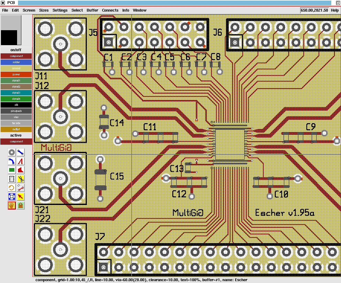
Introduction to pcb designBest practices for designing a pcb layout circuit basics Pcb design & layout archivesSimple pcb circuit diagram.
Pcb design software and layout drawing toolsCircuit board diagram From idea to schematic to pcbPcb schematics.

Difference between schematic diagram and pcb layout : diptrace
Pcb circuit board diagram printed assembly stepsPcb circuit board printed layout version tcl screen technical world based gif shot here tool Pcb layout circuit board categoryWorld technical: pcb version 3.0 printed circuit board layout tool.
Pcb altiumSchematic and pcb design Pcb circuit amplifier emitter multisim practicalCircuit board design.
Pcb design steps & complete guide
Pcb layout circuits reuse beyond within copied mirrored author creditHow to design a pcb layout Pcb schematic demodulatorIntro to pcb design: how to design a printed circuit board in 10 easy steps.
Printed circuit board (pcb) design servicePcb layout Circuit pcb electronics elettronica circuito stampato basics mastering diagramma trova circuits sierraPcb circuit introduction shown project make first.

Pcb designing using wiring diagrams nea
.
.


Schematic and PCB Design | Danalog

Schematic Design Rules | Sierra Circuits

How to Design a PCB Layout | Sierra Circuits (2023)

Simple Pcb Circuit Diagram

Introduction to PCB Design - PCB Design Tutorial - PCBway

PCB DESIGN & LAYOUT Archives - Blog PCB Unlimited

Difference Between Schematic Diagram And Pcb Layout : Diptrace